Mark Zuckerberg, CEO of Meta, has hired three researchers from OpenAI to bolster his company’s work on artificial intelligence. This strategic move aims to guide Meta Platforms through its current AI challenges. The social-media corporation brought aboard Lucas Beyer, Alexander Kolesnikov, and Xiaohua Zhai, all of whom previously held positions at OpenAI’s branch in Zurich, as per sources privy to this information. These individuals established OpenAI’s location in Zurich towards the end of last year. Prior to their time at OpenAI, they collaborated closely within Google DeepMind, which is the organization’s artificial intelligence division. A representative from OpenAI verified that the three scientists have departed from the organization. Zuckerberg has been on an intense recruiting drive To correct the company’s AI initiatives following the underwhelming reception of its most recent model, he has sometimes proposed giving researchers up to $100 million to become part o...
The dimensions of silicon wafers might not be what you imagine, and those incredibly tiny "3nm" and "2nm" chips you frequently hear about? They function more as promotional labels rather than precise measurements.
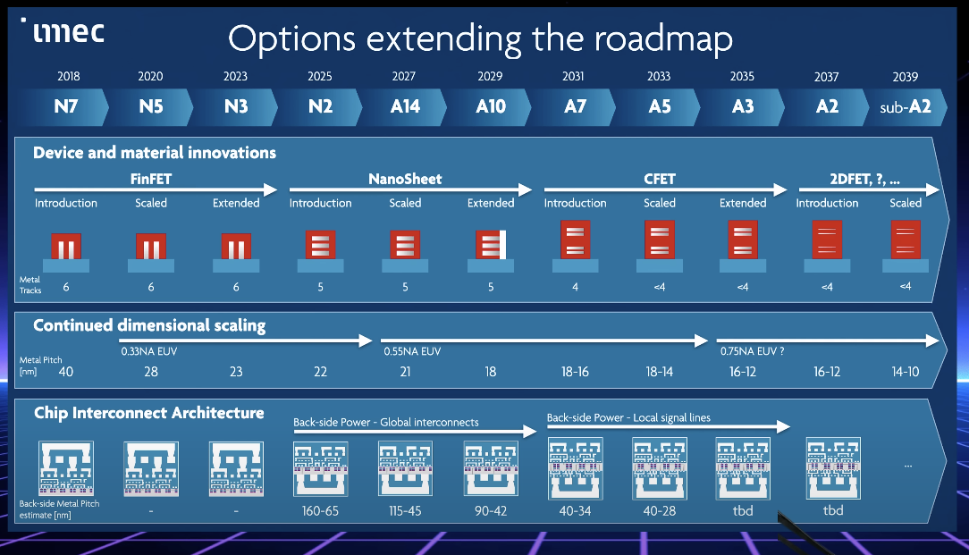
The most recent forecasts from the Interuniversity Microelectronics Centre (IMEC) have been dissected by YouTuber TechTechPotato , outlines the present timeline for TSMC's 2nm chipsets , as well as Intel Foundry's 18A and 14A manufacturing process technologies , where A14 chips with 1.4nm technology are anticipated for release in 2027, followed by the A10 processors using the 1nm process node scheduled for 2029. IMEC's predictions Even underscore the potential for manufacturing 0.2mm silicon as soon as 2039.
Actually, these figures significantly diverge from the actual, quantifiable transistors present on a semiconductor wafer. We might have to wait until sometime around the late 2030s just to surpass the 10nm threshold. The reasons for this are as follows.
The silicon wafers may not be as tiny as one might imagine despite being at the 2nm scale.
The 2-nanometer and 1.8 nanometer silicon technologies being developed by TSMC and Intel do not utilize wafers that are 2 nanometers thick.
2 nanometers is likewise not the distance between two transistors on the wafer.
Chip makers typically identify silicon wafers according to the smallest feature size that can be produced on the wafer’s surface during manufacturing. Currently, this dimension generally corresponds to the name Rather than being based on any specific physical characteristic of the chip, this depends on the process node.
Actually, starting around 1997, The naming of silicon processing nodes has been misleading. Intel’s 250nm process node technically featured a gate length of 200nm. This pattern of underreporting continued at Intel until 2011, when the silicon process nodes were reduced to 22nm, although their actual gate length was 26nm.
In 2018, TSMC and Samsung both embraced "perceptual marketing" for their silicon using the 7nm process nodes, which had a comparable gate length to Intel’s 10nm chips.
And the misunderstanding has only escalated further from there.
If you seek concrete physical dimensions for the present 3-nanometer chips, their gate length measures between 16 and 18 nanometers, with a metal pitch around 23 nanometers.
Therefore, despite all the discussion about 2 nm and 3 nm technology, we probably won't witness genuine 10-nanometer silicon before the anticipated sub-A2 chip generation around 2039, as forecasted by IMEC.
The size of wafers and Moore's Law are closely interconnected.
To recap briefly, Moore’s Law refers to the trend in semiconductor engineering where the count of transistors on an integrated circuit tends to double approximately every twenty-four months. With advancements making silicon chips increasingly compact, this progression occurs until fundamental physical limitations come into play.
Unlike what its title suggests, Moore’s Law is not truly a law, but more of an insight into chip fabrication. Ultimately, transistors can shrink only so far before overheating poses a significant challenge for engineers designing these components.

Nvidia's CEO, Jensen Huang, has been against the idea of continuing the Moore's Law trend largely due to the higher thermal constraints of discrete graphics cards, while CPUs like Intel's Lunar Lake chipset offers more space for development. (or reduce, in this case).
However, considering IMEC’s clarification regarding the actual dimensions of silicon wafers along with anticipated advancements in chip interconnection design and transistor technology, extending Moore's Law doesn’t seem unfeasible. While predicting whether this progression will sustain beyond the coming ten years remains uncertain, present forecasts suggest it could be within reach.
As mentioned, the possible count of transistors within those below A2 (10nm Lg) chipset range is remarkable. For instance, the present Intel Core Ultra 9 285K boasts approximately 18 billion transistors. The sub-A2 chipsets might contain approximately 300 billion transistors by 2039. .
More from Laptop Mag
- The upcoming PlayStation and Xbox consoles might share an unexpected feature — but is this a positive development?
- The GeForce RTX 5050 introduces cutting-edge gaming technology to mainstream consumers, available in Blackwell laptops for as low as $999.
- Intel's potent 2026 Nova Lake processor might make standalone graphics cards unnecessary, and it has recently been found in top-tier laptops.
Enjoying this piece? To read more articles like this one, follow us on MSN by tapping the +Follow button at the top of this page.